
As imagens são apenas para referência. Consulte as especificações do produto
Pedidos acima de
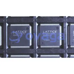
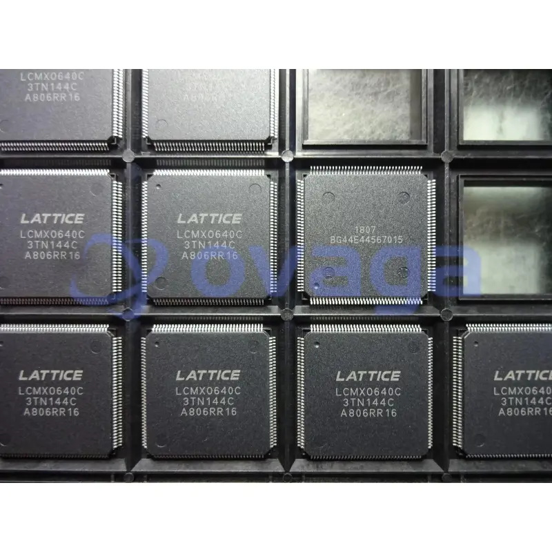
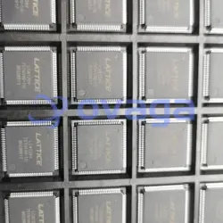
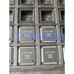
$5000LATTICE LCMXO640C-3TN144C
Programmable FPGA with 640 LUTs and 113 I/O


Marcas: LATTICE
Parte do fabricante #: LCMXO640C-3TN144C
Ficha de dados: LCMXO640C-3TN144C Ficha de dados (PDF)
Pacote/Caso: TQFP144
Tipo de Produto: FPGAs (Field Programmable Gate Array)
Status RoHS:
Condição de estoque: 9.458 peças, novo original
Warranty: 1 Year Ovaga Warranty - Find Out More
0
1
LCMXO640C-3TN144C Descrição geral
When it comes to programmability and flexibility, the LCMXO640C-3TN144C FPGA stands out with its field programmable gate array technology. This FPGA offers engineers the ability to customize their logic functions according to specific application requirements. With the 640 LUTs onboard, designers have ample resources to implement complex algorithms and logic operations efficiently
Características
- Non-volatile, Infinitely Reconfigurable
- Instant-on – powers up in microseconds
- Single chip, no external configuration memory
- required
- Excellent design security, no bit stream to
- intercept
- Reconfigure SRAM based logic in milliseconds
- SRAM and non-volatile memory programmable
- through JTAG port
- Supports background programming of
- non-volatile memory
- Sleep Mode
- Allows up to 100x static current reduction
- TransFR™ Reconfiguration (TFR)
- In-field logic update while system operates
- High I/O to Logic Density
- 256 to 2280 LUT4s
- 73 to 271 I/Os with extensive package options
- Density migration supported
- Lead free/RoHS compliant packaging
- Embedded and Distributed Memory
- Up to 27.6 Kbits sysMEM™ Embedded Block
- RAM
- Up to 7.5 Kbits distributed RAM
- Dedicated FIFO control logic
- Flexible I/O Buffer
- Programmable sysIO™ buffer supports wide
- range of interfaces:
- − LVCMOS 3.3/2.5/1.8/1.5/1.2
- − LVTTL
- − PCI
- − LVDS, Bus-LVDS, LVPECL, RSDS
- sysCLOCK™ PLLs
- Up to two analog PLLs per device
- Clock multiply, divide, and phase shifting
- System Level Support
- IEEE Standard 1149.1 Boundary Scan
- Onboard oscillator
- Devices operate with 3.3V, 2.5V, 1.8V or 1.2V
- power supply
- IEEE 1532 compliant in-system programming

Especificações
| Parâmetro | Valor | Parâmetro | Valor |
|---|---|---|---|
| Product Category | FPGA - Field Programmable Gate Array | RoHS | Details |
| Series | LCMXO640C | Number of Logic Elements | 640 LE |
| Adaptive Logic Modules - ALMs | 320 ALM | Embedded Memory | 0 bit |
| Number of I/Os | 113 I/O | Supply Voltage - Min | 1.71 V |
| Supply Voltage - Max | 3.465 V | Minimum Operating Temperature | 0 C |
| Maximum Operating Temperature | + 85 C | Mounting Style | SMD/SMT |
| Package / Case | CSBGA-144 | Brand | Lattice |
| Distributed RAM | 6.1 kbit | Height | 1.4 mm |
| Length | 20 mm | Maximum Operating Frequency | 500 MHz |
| Moisture Sensitive | Yes | Number of Logic Array Blocks - LABs | 80 LAB |
| Operating Supply Current | 17 mA | Operating Supply Voltage | 1.8 V/2.5 V/3.3 V |
| Product Type | FPGA - Field Programmable Gate Array | Factory Pack Quantity | 60 |
| Subcategory | Programmable Logic ICs | Total Memory | 6.1 kbit |
| Width | 20 mm |
Envio
| Tipo de envio | Taxa de envio | Tempo de espera | |
|---|---|---|---|
 |
DHL | $20.00-$40.00 (0.50 KG) | 2-5 dias |
 |
FedEx | $20.00-$40.00 (0.50 KG) | 2-5 dias |
 |
UPS | $20.00-$40.00 (0.50 KG) | 2-5 dias |
 |
TNT | $20.00-$40.00 (0.50 KG) | 2-5 dias |
 |
EMS | $20.00-$40.00 (0.50 KG) | 2-5 dias |
 |
CORREIO AÉREO REGISTADO | $20.00-$40.00 (0.50 KG) | 2-5 dias |
Tempo de processamento: A taxa de envio depende de diferentes zonas e países.
Pagamento
| Termos de pagamento | Taxa de mão | |
|---|---|---|
 |
Transferência bancária | cobrar taxa bancária de US$ 30,00. |
 |
PayPal | cobrar taxa de serviço de 4,0%. |
 |
Cartão de crédito | cobrar taxa de serviço de 3,5%. |
 |
Western Union | charge US.00 banking fee. |
 |
Grama de dinheiro | cobrar taxa bancária de US$ 0,00. |
Garantias
1.Os componentes eletrônicos que você compra incluem garantia de 365 dias, garantimos a qualidade do produto.
2. se alguns dos itens que você recebeu não forem de qualidade perfeita, providenciaremos seu reembolso ou substituição com responsabilidade. Mas os itens devem permanecer em sua condição original.
Embalagem
-

Etapa1 :produtos
-

Etapa2 :Embalagem a vácuo
-

Etapa3 :Saco antiestático
-

Etapa4 :Embalagem individual
-

Etapa5 :Caixas de embalagem
-

Etapa6 :etiqueta de envio com código de barras


Todos os produtos serão embalados em saco antiestático. Envio com proteção antiestática ESD.
Fora da etiqueta da embalagem ESD serão utilizadas as informações da nossa empresa: Número da peça, marca e quantidade.
Iremos inspecionar todas as mercadorias antes do envio, garantir que todos os produtos estejam em boas condições e garantir que as peças sejam novas folhas de dados originais.
Depois que todas as mercadorias forem garantidas sem problemas na pós-embalagem, embalaremos com segurança e enviaremos por expresso global. Apresenta excelente resistência a perfurações e rasgos, além de boa integridade de vedação.


Part points
-
The LCMXO640C-3TN144C is a programmable logic device (PLD) chip manufactured by Lattice Semiconductor. It belongs to the Lattice XO2 family of FPGAs and has 640 Look-Up Tables (LUTs) and 640 logical registers. With a density of 640 LUTs, this chip offers a cost-effective and low-power solution for a variety of applications such as consumer electronics, industrial automation, and communication devices.
-
Features
LCMXO640C-3TN144C is a low-power, non-volatile PLD (Programmable Logic Device) with a capacity of 640 Look-Up Tables (LUTs) and 32640 bits of RAM. It operates with a supply voltage of 3.3V and offers 144-pin TQFP packaging. Additionally, it features an internal oscillator and programmable routing to cater to various digital designs. -
Pinout
The LCMXO640C-3TN144C is a Field-Programmable Gate Array (FPGA) with a pin count of 144. It functions as a programmable logic device that can be configured to perform various digital functions. -
Manufacturer
The manufacturer of the LCMXO640C-3TN144C is Lattice Semiconductor Corporation. It is a semiconductor company that specializes in the design and manufacture of programmable logic devices, including field-programmable gate arrays (FPGAs) and complex programmable logic devices (CPLDs). -
Application Field
The LCMXO640C-3TN144C can be used in various application areas such as portable consumer electronics, industrial automation, automotive systems, and communication devices. -
Package
The LCMXO640C-3TN144C chip has a package type of TQFP (Thin Quad Flat Package), a form of leaded surface mount, and a size of 14 x 14 mm.


Oferecemos produtos de alta qualidade, serviço atencioso e garantia pós-venda
-

Temos produtos ricos que podem atender às suas diversas necessidades.
-

A quantidade mínima de pedido começa em 1 unidade.
-

A menor taxa de envio internacional começa em US$ 0,00
-

365 dias de garantia de qualidade para todos os produtos