

As imagens são apenas para referência. Consulte as especificações do produto
Pedidos acima de
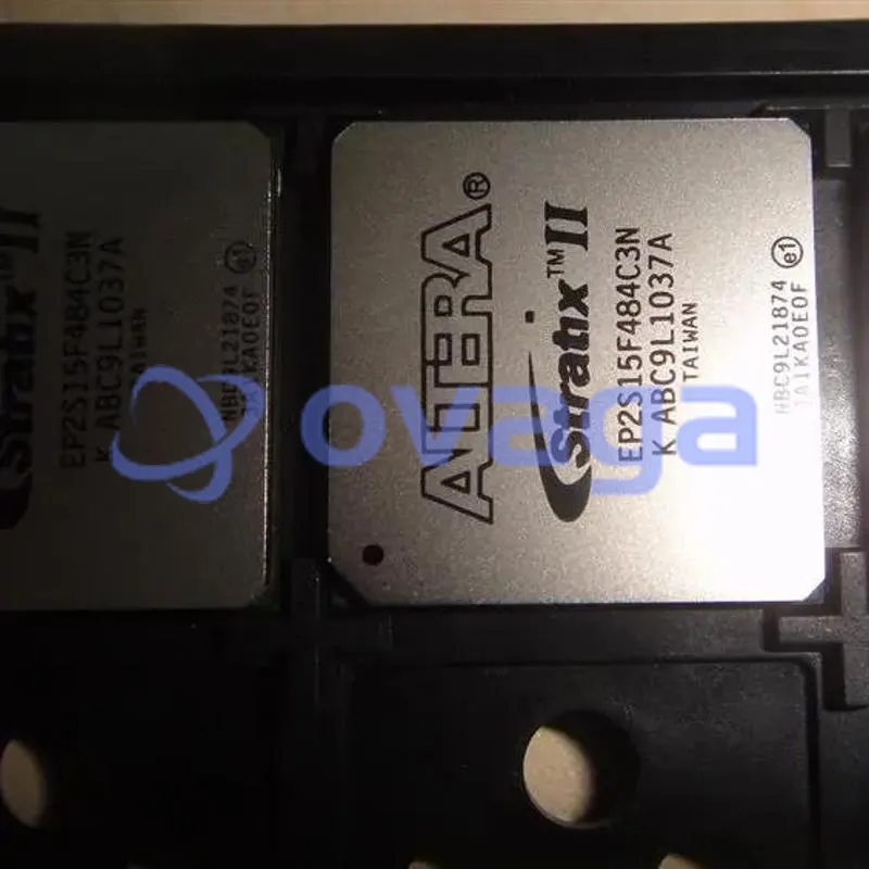
$5000Intel EP2S15F484C3N
FC-FBGA packaged EP2S15F484C3N FPGA, part of the Stratix® II Family with a maximum frequency of 816.99MHz


Marcas: Intel
Parte do fabricante #: EP2S15F484C3N
Ficha de dados: EP2S15F484C3N Ficha de dados (PDF)
Pacote/Caso: FBGA-484
Tipo de Produto: FPGAs (Field Programmable Gate Array)
Status RoHS:
Condição de estoque: 9.614 peças, novo original
Warranty: 1 Year Ovaga Warranty - Find Out More
0
1
EP2S15F484C3N Descrição geral
The EP2S15F484C3N is a high-performance FPGA Logic IC that belongs to the renowned Stratix II series. Boasting 342 I/Os and advanced clock management features such as PLL and DLL, this IC offers exceptional versatility and functionality. It operates at a 3.3V I/O supply voltage and can withstand temperatures from 0°C to +85°C, making it suitable for diverse operating environments. With a FBGA logic case style and 484 pins, it is designed for secure and efficient integration into various electronic designs. Furthermore, this product is RoHS compliant, reflecting its adherence to strict environmental standards
Características
- 15,600 to 179,400 equivalent LEs New and innovative adaptive logic module (ALM), the basic building block of the Stratix II architecture, maximizes performance and resource usage efficiency Up to 9,383,040 RAM bits (1,172,880 bytes) available without reducing logic resources TriMatrix memory consisting of three RAM block sizes to implement true dual-port memory and first-in first-out (FIFO) buffers High-speed DSP blocks provide dedicated implementation of multipliers (at up to 450 MHz), multiply-accumulate functions, and finite impulse response (FIR) filters Up to 16 global clocks with 24 clocking resources per device region Clock control blocks support dynamic clock network enable/disable, which allows clock networks to power down to reduce power consumption in user mode Up to 12 PLLs (four enhanced PLLs and eight fast PLLs) per device provide spread spectrum, programmable bandwidth, clock switchover, real-time PLL reconfiguration, and advanced multiplication and phase shifting Support for numerous single-ended and differential I/O standards High-speed differential I/O support with DPA circuitry for 1-Gbps performance Support for high-speed networking and communications bus standards including Parallel RapidIO, SPI-4 Phase 2 (POS-PHY Level 4), HyperTransport™ technology, and SFI-4 Support for high-speed external memory, including DDR and DDR2 SDRAM, RLDRAM II, QDR II SRAM, and SDR SDRAM Support for multiple intellectual property megafunctions from Altera MegaCore® functions and Altera Megafunction Partners Program (AMPPSM) megafunctions Support for design security using configuration bitstream encryption Support for remote configuration updates
Especificações
| Parâmetro | Valor | Parâmetro | Valor |
|---|---|---|---|
| Product Status | Obsolete | Programmabe | Not Verified |
| Number of LABs/CLBs | 780 | Number of Logic Elements/Cells | 15600 |
| Total RAM Bits | 419328 | Number of I/O | 342 |
| Number of Gates | - | Voltage - Supply | 1.15V ~ 1.25V |
| Mounting Type | Surface Mount | Operating Temperature | 0°C ~ 85°C (TJ) |
| Package / Case | 484-BBGA |
Envio
| Tipo de envio | Taxa de envio | Tempo de espera | |
|---|---|---|---|
 |
DHL | $20.00-$40.00 (0.50 KG) | 2-5 dias |
 |
FedEx | $20.00-$40.00 (0.50 KG) | 2-5 dias |
 |
UPS | $20.00-$40.00 (0.50 KG) | 2-5 dias |
 |
TNT | $20.00-$40.00 (0.50 KG) | 2-5 dias |
 |
EMS | $20.00-$40.00 (0.50 KG) | 2-5 dias |
 |
CORREIO AÉREO REGISTADO | $20.00-$40.00 (0.50 KG) | 2-5 dias |
Tempo de processamento: A taxa de envio depende de diferentes zonas e países.
Pagamento
| Termos de pagamento | Taxa de mão | |
|---|---|---|
 |
Transferência bancária | cobrar taxa bancária de US$ 30,00. |
 |
PayPal | cobrar taxa de serviço de 4,0%. |
 |
Cartão de crédito | cobrar taxa de serviço de 3,5%. |
 |
Western Union | charge US.00 banking fee. |
 |
Grama de dinheiro | cobrar taxa bancária de US$ 0,00. |
Garantias
1.Os componentes eletrônicos que você compra incluem garantia de 365 dias, garantimos a qualidade do produto.
2. se alguns dos itens que você recebeu não forem de qualidade perfeita, providenciaremos seu reembolso ou substituição com responsabilidade. Mas os itens devem permanecer em sua condição original.
Embalagem
-

Etapa1 :produtos
-

Etapa2 :Embalagem a vácuo
-

Etapa3 :Saco antiestático
-

Etapa4 :Embalagem individual
-

Etapa5 :Caixas de embalagem
-

Etapa6 :etiqueta de envio com código de barras


Todos os produtos serão embalados em saco antiestático. Envio com proteção antiestática ESD.
Fora da etiqueta da embalagem ESD serão utilizadas as informações da nossa empresa: Número da peça, marca e quantidade.
Iremos inspecionar todas as mercadorias antes do envio, garantir que todos os produtos estejam em boas condições e garantir que as peças sejam novas folhas de dados originais.
Depois que todas as mercadorias forem garantidas sem problemas na pós-embalagem, embalaremos com segurança e enviaremos por expresso global. Apresenta excelente resistência a perfurações e rasgos, além de boa integridade de vedação.


Part points
-
The EP2S15F484C3N chip is a field-programmable gate array (FPGA) designed by Altera. It belongs to the Stratix II family and is manufactured using a 90nm process. With 15,408 logic elements, 588 embedded multipliers, and 1.4 Mbits of SRAM, this chip is versatile and powerful. It is widely used in various applications, including telecommunications, aerospace, and industrial automation.
-
Equivalent
The equivalent products of EP2S15F484C3N chip include EP2S15F484C5N and EP2S15F484I5N. -
Features
The EP2S15F484C3N is a field programmable gate array (FPGA) from the Stratix II family by Altera. It offers 15,360 logic elements, 552 embedded memory blocks, and 266 I/O pins. It operates at 1.2V and has a maximum frequency of 600 MHz. It is designed for high-performance applications, such as wireless communication and video processing. -
Pinout
The EP2S15F484C3N is an FPGA (Field-Programmable Gate Array) device from the Cyclone II series by Intel (formerly Altera). It has a pin count of 484 pins and offers various functions such as logic and memory elements, as well as digital signal processing capabilities. -
Manufacturer
The EP2S15F484C3N is manufactured by Altera Corporation. It is an American company specializing in semiconductors and programming solutions. Altera focuses on developing and manufacturing programmable logic devices such as field-programmable gate arrays (FPGAs) and complex programmable logic devices (CPLDs). -
Application Field
The EP2S15F484C3N is a field-programmable gate array (FPGA) device. It is commonly used in various application areas such as telecommunications, networking, video and image processing, high-performance computing, industrial automation, and automotive electronics. With its flexibility and reconfigurable nature, it can be used in a wide range of applications that require high-speed data processing and complex digital logic implementation. -
Package
The EP2S15F484C3N chip is packaged in a 484-pin FineLine BGA (Ball Grid Array) package. It is in form factor C3N and has a 15mm x 15mm size.


Oferecemos produtos de alta qualidade, serviço atencioso e garantia pós-venda
-

Temos produtos ricos que podem atender às suas diversas necessidades.
-

A quantidade mínima de pedido começa em 1 unidade.
-

A menor taxa de envio internacional começa em US$ 0,00
-

365 dias de garantia de qualidade para todos os produtos


