

As imagens são apenas para referência. Consulte as especificações do produto
ON NC7WV07P6X
Buffer, Non-Inverting 2 Element 1 Bit per Element Open Drain Output SC-88 (SC-70-6)


Marcas: ON Semiconductor, LLC
Parte do fabricante #: NC7WV07P6X
Ficha de dados: NC7WV07P6X Datasheet (PDF)
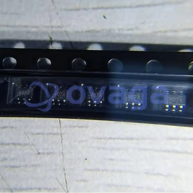
Pacote/Caso: SC-70-6
Tipo de Produto: CIs lógicos
Status RoHS:
Condição de estoque: 3547 peças, novo original
Warranty: 1 Year Ovaga Warranty - Find Out More
0
1
Adicionar à lista técnicaNC7WV07P6X Descrição geral
The NC7WV07 is a dual buffer with open drain output from ON Semiconductor's Ultra Low Power-A series of TinyLogic®. ULP-A is ideal for applications that require extreme high speed, high drive and low power. This product is designed for a wide low voltage operating range (0.9V to 3.6V VCC) and applications that require more drive and speed than the TinyLogic ULP series, but still offer best in class low power operation.
The NC7WV07 is uniquely designed for optimized power and speed, and is fabricated with an advanced CMOS technology to achieve high-speed operation while maintaining low CMOS power dissipation.
Características
- 0.9V to 3.6V VCC supply operation
- 3.6V overvoltage tolerant I/O's at VCC from 0.9V to 3.6V
- Extremely High Speed tPD1.0 ns typ for 2.7V to 3.6V VCC1.2 ns typ for 2.3V to 2.7V VCC2.0 ns typ for 1.65V to 1.95V VCC3.2 ns typ for 1.4V to 1.6V VCC6.0 ns typ for 1.1V to 1.3V VCC13.0 ns typ for 0.9V VCC
- Power-Off high impedance inputs and outputs
- High Static Drive (IOH/IOL)±24 mA @ 3.00V VCC±18 mA @ 2.30V VCC±6 mA @ 1.65V VCC±4 mA @ 1.4V VCC±2 mA @ 1.1V VCC±0.1 mA @ 0.9V VCC
- Uses patented Quiet Series™ noise/EMI reduction circuitry
- Ultra small MicroPak™ leadfree package
- Ultra low dynamic power
Aplicativo
- This product is general usage and suitable for many different applications.
Especificações
| Parâmetro | Valor | Parâmetro | Valor |
|---|---|---|---|
| Source Content uid | NC7WV07P6X | Pbfree Code | Yes |
| Part Life Cycle Code | Active | Ihs Manufacturer | ONSEMI |
| Package Description | SC-88, 6 PIN | Manufacturer Package Code | 419AD |
| Reach Compliance Code | compliant | HTS Code | 8542.39.00.01 |
| Factory Lead Time | 75 Weeks, 5 Days | Samacsys Manufacturer | onsemi |
| Family | AUP/ULP/V | JESD-30 Code | R-PDSO-G6 |
| Logic IC Type | BUFFER | Moisture Sensitivity Level | 1 |
| Number of Functions | 2 | Number of Inputs | 1 |
| Number of Terminals | 6 | Output Characteristics | OPEN-DRAIN |
| Package Body Material | PLASTIC/EPOXY | Package Code | TSSOP |
| Package Equivalence Code | TSSOP6,.08 | Package Shape | RECTANGULAR |
| Package Style | SMALL OUTLINE, THIN PROFILE, SHRINK PITCH | Packing Method | TR |
| Peak Reflow Temperature (Cel) | 260 | Schmitt Trigger | NO |
| Surface Mount | YES | Technology | CMOS |
| Terminal Finish | NICKEL PALLADIUM GOLD | Terminal Form | GULL WING |
| Terminal Position | DUAL | Time@Peak Reflow Temperature-Max (s) | 30 |
| feature-logic-family | WV | feature-logic-function | Buffer/Driver |
| feature-number-of-elements-per-chip | 2 | feature-process-technology | CMOS |
| feature-maximum-low-level-output-current-ma | 24 | feature-output-type | Open Drain |
| feature-minimum-operating-supply-voltage-v | 0.9 | feature-maximum-operating-supply-voltage-v | 3.6 |
| feature-maximum-high-level-output-current-ma | -24 | feature-packaging | Tape and Reel |
| feature-rad-hard | feature-pin-count | 6 | |
| feature-supplier-package | SC-70 | feature-standard-package-name1 | SOT |
| feature-cecc-qualified | No | feature-esd-protection | |
| feature-military | No | feature-aec-qualified | No |
| feature-aec-qualified-number | feature-auto-motive | No | |
| feature-p-pap | No | feature-eccn-code | EAR99 |
| feature-svhc | No |
Envio
| Tipo de envio | Taxa de envio | Tempo de espera | |
|---|---|---|---|
 |
DHL | $20.00-$40.00 (0.50 KG) | 2-5 dias |
 |
FedEx | $20.00-$40.00 (0.50 KG) | 2-5 dias |
 |
UPS | $20.00-$40.00 (0.50 KG) | 2-5 dias |
 |
TNT | $20.00-$40.00 (0.50 KG) | 2-5 dias |
 |
EMS | $20.00-$40.00 (0.50 KG) | 2-5 dias |
 |
CORREIO AÉREO REGISTADO | $20.00-$40.00 (0.50 KG) | 2-5 dias |
Tempo de processamento: A taxa de envio depende de diferentes zonas e países.
Pagamento
| Termos de pagamento | Taxa de mão | |
|---|---|---|
 |
Transferência bancária | cobrar taxa bancária de US$ 30,00. |
 |
PayPal | cobrar taxa de serviço de 4,0%. |
 |
Cartão de crédito | cobrar taxa de serviço de 3,5%. |
 |
Western Union | charge US.00 banking fee. |
 |
Grama de dinheiro | cobrar taxa bancária de US$ 0,00. |
Garantias
1.Os componentes eletrônicos que você compra incluem garantia de 365 dias, garantimos a qualidade do produto.
2. se alguns dos itens que você recebeu não forem de qualidade perfeita, providenciaremos seu reembolso ou substituição com responsabilidade. Mas os itens devem permanecer em sua condição original.
Embalagem
-

Etapa1 :produtos
-

Etapa2 :Embalagem a vácuo
-

Etapa3 :Saco antiestático
-

Etapa4 :Embalagem individual
-

Etapa5 :Caixas de embalagem
-

Etapa6 :etiqueta de envio com código de barras


Todos os produtos serão embalados em saco antiestático. Envio com proteção antiestática ESD.
Fora da etiqueta da embalagem ESD serão utilizadas as informações da nossa empresa: Número da peça, marca e quantidade.
Iremos inspecionar todas as mercadorias antes do envio, garantir que todos os produtos estejam em boas condições e garantir que as peças sejam novas folhas de dados originais.
Depois que todas as mercadorias forem garantidas sem problemas na pós-embalagem, embalaremos com segurança e enviaremos por expresso global. Apresenta excelente resistência a perfurações e rasgos, além de boa integridade de vedação.


Part points
-
The NC7WV07P6X chip is a triple buffer gate that can be used for level shifting signals in various electronic circuits. It has three inputs and three outputs and operates at a supply voltage of 1.65V to 5.5V. The chip is designed to provide high-speed signal buffering while consuming very low power, making it suitable for applications in portable devices and battery-powered systems.
-
Equivalent
There aren't any exact equivalent products to the NC7WV07P6X chip. However, some similar alternatives you may consider are the SN74LV07A, TC7WG07FK, and HCT07 chips, as they have similar functionalities and specifications. -
Features
The NC7WV07P6X is a dual buffer/line driver that operates from rail-to-rail voltage signals with a wide operating voltage range. It offers low power consumption, high-speed operation, and is designed with Schmitt-trigger inputs to provide noise immunity. It also has balanced input and output characteristics and supports overvoltage-tolerant input levels, making it suitable for various applications. -
Pinout
The NC7WV07P6X is a single logic gate with an open-drain output. It has a pin count of 6, which includes one input pin, one output pin, and four power supply/GND pins. The open-drain output allows for bi-directional signal transmission and is commonly used for level shifting applications. -
Manufacturer
The manufacturer of the NC7WV07P6X is ON Semiconductor. ON Semiconductor is a multinational company specializing in the design and production of semiconductors and integrated circuits for various industries, including automotive, communications, computing, and consumer electronics. -
Application Field
The NC7WV07P6X is a voltage-level translator used for translating voltage levels between different logic families. It can be applied in various applications such as battery-powered portable devices, mobile phones, digital cameras, and other electronics requiring voltage translation between different logic levels. -
Package
The NC7WV07P6X chip has a package type of SC-70, a form of SMD (Surface Mount Device), and a size of 2.00mm x 2.10mm x 1.20mm.


Ficha de dados PDF
Oferecemos produtos de alta qualidade, serviço atencioso e garantia pós-venda
-

Temos produtos ricos que podem atender às suas diversas necessidades.
-

A quantidade mínima de pedido começa em 1 unidade.
-

A menor taxa de envio internacional começa em US$ 0,00
-

365 dias de garantia de qualidade para todos os produtos


We will definitely be purchasing from Ovaga in the future.