


As imagens são apenas para referência. Consulte as especificações do produto
Pedidos acima de
$5000
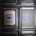
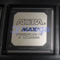
Altera EP2C70F896C6N

With 896 pins and housed in a fine-pitch ball grid array (FBGA) package


Marcas: Altera
Parte do fabricante #: EP2C70F896C6N
Ficha de dados: EP2C70F896C6N Ficha de dados (PDF)
Pacote/Caso: FBGA-896
Status RoHS:
Condição de estoque: 2.399 peças, novo original
Tipo de Produto: FPGAs (Field Programmable Gate Array)
Warranty: 1 Year Ovaga Warranty - Find Out More
0
1
*Todos os preços estão em USD
| Quantidade | Preço unitário | Preço Externo |
|---|---|---|
| 1 | $2090,893 | $2090,893 |
| 189 | $834,280 | $157678,920 |
| 513 | $806,402 | $413684,226 |
| 999 | $792,626 | $791833,374 |
Em estoque: 2.399 PCS
EP2C70F896C6N Descrição geral
The EP2C70F896C6N FPGA, a cornerstone of Altera's legacy now seamlessly integrated into Intel's portfolio, is a testament to relentless innovation in the realm of programmable logic devices. Boasting a formidable arsenal of 70,000 logic elements and 896 pins, it stands as a pinnacle of engineering prowess, designed to excel in mission-critical applications demanding both speed and efficiency. With its finely tuned architecture and comprehensive feature set—including embedded memory, DSP slices, and PLLs—it delivers unparalleled performance across diverse domains. Whether deployed in telecommunications infrastructure or automotive control systems, its adaptability and reconfigurability empower developers to push the boundaries of what's possible, ushering in a new era of computational agility and efficiency

Especificações
| Parâmetro | Valor | Parâmetro | Valor |
|---|---|---|---|
| feature-family-name | Cyclone® II | feature-process-technology | 90nm |
| feature-maximum-number-of-user-i-os | 622 | feature-number-of-registers | |
| feature-device-logic-cells | 68416 | feature-device-system-gates | |
| feature-number-of-multipliers | 150 (18x18) | feature-program-memory-type | SRAM |
| feature-ram-bits-kbit | 1125 | feature-total-number-of-block-ram | 250 |
| feature-ethernet-macs | feature-supported-ip-core | 32/64-bit PCI-X bus Master/Target interface Core, 66/100/133Mhz|10 Gigabit Ethernet MAC|SpeedView Enabled JPEG Encoder (SVE-JPEG-E)|V1 ColdFire|Viterbi Compiler, Low-Speed/Hybrid Serial Decoder | |
| feature-supported-ip-core-manufacture | Altera/Freescale/CAST, Inc/MorethanIP/PLDA | feature-maximum-number-of-serdes-channels | |
| feature-device-logic-units | 68416 | feature-device-number-of-dlls-plls | 4 |
| feature-transceiver-blocks | feature-transceiver-speed-gbps | ||
| feature-dedicated-dsp | feature-pci-blocks | ||
| feature-programmability | No | feature-maximum-internal-frequency-mhz | 500 |
| feature-speed-grade | 6 | feature-giga-multiply-accumulates-per-second | |
| feature-differential-i-o-standards-supported | PCI-X|LVDS | feature-single-ended-i-o-standards-supported | PCI-X|LVDS |
| feature-external-memory-interface | QDR II+SRAM|DDR SDRAM | feature-minimum-operating-supply-voltage-v | 1.15 |
| feature-maximum-operating-supply-voltage-v | 1.25 | feature-packaging | |
| feature-rohs | feature-rad-hard | ||
| feature-pin-count | 896 | feature-supplier-package | FBGA |
| feature-standard-package-name1 | BGA | feature-cecc-qualified | No |
| feature-esd-protection | feature-escc-qualified | ||
| feature-military | No | feature-aec-qualified | No |
| feature-aec-qualified-number | feature-auto-motive | No | |
| feature-p-pap | No | feature-eccn-code | 3A991 |
| feature-svhc | No |
Envio
| Tipo de envio | Taxa de envio | Tempo de espera | |
|---|---|---|---|
 |
DHL | $20.00-$40.00 (0.50 KG) | 2-5 dias |
 |
FedEx | $20.00-$40.00 (0.50 KG) | 2-5 dias |
 |
UPS | $20.00-$40.00 (0.50 KG) | 2-5 dias |
 |
TNT | $20.00-$40.00 (0.50 KG) | 2-5 dias |
 |
EMS | $20.00-$40.00 (0.50 KG) | 2-5 dias |
 |
CORREIO AÉREO REGISTADO | $20.00-$40.00 (0.50 KG) | 2-5 dias |
Tempo de processamento: A taxa de envio depende de diferentes zonas e países.
Pagamento
| Termos de pagamento | Taxa de mão | |
|---|---|---|
 |
Transferência bancária | cobrar taxa bancária de US$ 30,00. |
 |
PayPal | cobrar taxa de serviço de 4,0%. |
 |
Cartão de crédito | cobrar taxa de serviço de 3,5%. |
 |
Western Union | charge US.00 banking fee. |
 |
Grama de dinheiro | cobrar taxa bancária de US$ 0,00. |
Garantias
1.Os componentes eletrônicos que você compra incluem garantia de 365 dias, garantimos a qualidade do produto.
2. se alguns dos itens que você recebeu não forem de qualidade perfeita, providenciaremos seu reembolso ou substituição com responsabilidade. Mas os itens devem permanecer em sua condição original.
Embalagem
-

Etapa1 :produtos
-

Etapa2 :Embalagem a vácuo
-

Etapa3 :Saco antiestático
-

Etapa4 :Embalagem individual
-

Etapa5 :Caixas de embalagem
-

Etapa6 :etiqueta de envio com código de barras


Todos os produtos serão embalados em saco antiestático. Envio com proteção antiestática ESD.
Fora da etiqueta da embalagem ESD serão utilizadas as informações da nossa empresa: Número da peça, marca e quantidade.
Iremos inspecionar todas as mercadorias antes do envio, garantir que todos os produtos estejam em boas condições e garantir que as peças sejam novas folhas de dados originais.
Depois que todas as mercadorias forem garantidas sem problemas na pós-embalagem, embalaremos com segurança e enviaremos por expresso global. Apresenta excelente resistência a perfurações e rasgos, além de boa integridade de vedação.


Part points
-
The EP2C70F896C6N is a field-programmable gate array (FPGA) chip from Altera. It features 70,000 logic elements, over 2.1 million bits of RAM, and 343 user I/Os. The chip offers versatile programmability for a wide range of applications, such as telecommunications, automotive, and industrial automation.
-
Equivalent
Some equivalent products of the EP2C70F896C6N chip are Altera Cyclone II EP2C70F896C6, Intel Cyclone II EP2C70F896C6, and other FPGAs from the same family with similar specifications and features. These chips are commonly used for low-cost, entry-level FPGA development and prototyping. -
Features
EP2C70F896C6N is an FPGA device from Altera's Cyclone II family. It features 70,000 logic elements (LEs), 376 embedded memory blocks, 196 embedded 18 x 18 multipliers, and a maximum of 896 user I/Os. It operates on a 1.5V core voltage and supports various I/O standards. -
Pinout
The EP2C70F896C6N is a Field-Programmable Gate Array (FPGA) from Intel (formerly Altera) with a pin count of 896. It features 70,000 logic elements, 2060 kbits of embedded memory, and 220 DSP blocks. The device is used for implementing complex digital designs in various applications such as telecommunications, industrial automation, and signal processing. -
Manufacturer
The EP2C70F896C6N is manufactured by Intel Corporation, a multinational technology company known for its computing and communications products. They specialize in the design and production of processors, integrated circuits, and other hardware components used in a variety of devices and systems worldwide. -
Application Field
The EP2C70F896C6N is a field-programmable gate array (FPGA) commonly used in various applications such as industrial automation, automotive electronics, telecommunications, and aerospace. Its high processing power, programmability, and parallel processing capabilities make it ideal for applications requiring high performance, low latency, and reliability. -
Package
The EP2C70F896C6N chip is a Field Programmable Gate Array (FPGA) in an FBGA (Fine Pitch Ball Grid Array) package. It is in the form of a silicon chip, and the size is 27 x 27 mm with a 896-ball grid array (27 x 27, 0.8mm pitch).


Oferecemos produtos de alta qualidade, serviço atencioso e garantia pós-venda
-

Temos produtos ricos que podem atender às suas diversas necessidades.
-

A quantidade mínima de pedido começa em 1 unidade.
-

A menor taxa de envio internacional começa em US$ 0,00
-

365 dias de garantia de qualidade para todos os produtos


