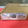


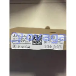
As imagens são apenas para referência. Consulte as especificações do produto
TI UCC21520DWR

5.7kVrms, 4A/6A dual-channel isolated gate driver w/ dual input, disable pin, 8V UVLO in DW package


Marcas: TI
Parte do fabricante #: UCC21520DWR
Ficha de dados: UCC21520DWR Ficha de dados (PDF)
Pacote/Caso: SOIC-16
Status RoHS:
Condição de estoque: 9372 peças, novo original
Tipo de Produto: Galvanically Isolated Gate Drivers
Warranty: 1 Year Ovaga Warranty - Find Out More
0
1
*Todos os preços estão em USD
| Quantidade | Preço unitário | Preço Externo |
|---|---|---|
| 1 | $1,307 | $1,307 |
| 10 | $1,087 | $10,870 |
| 30 | $0,964 | $28,920 |
| 100 | $0,826 | $82,600 |
| 500 | $0,766 | $383,000 |
| 1000 | $0,739 | $739,000 |
In Stock:9372 PCS
UCC21520DWR Descrição geral
The UCC21520 and the UCC21520A are isolated dual-channel gate drivers with 4-A source and 6-A sink peak current. It is designed to drive power MOSFETs, IGBTs, and SiC MOSFETs up to 5-MHz with best-in-class propagation delay and pulse-width distortion.
The input side is isolated from the two output drivers by a 5.7-kVRMS reinforced isolation barrier, with a minimum of 100-V/ns common-mode transient immunity (CMTI). Internal functional isolation between the two secondary-side drivers allows a working voltage of up to 1500 VDC.
Every driver can be configured as two low-side drivers, two high-side drivers, or a half-bridge driver with programmable dead time (DT). A disable pin shuts down both outputs simultaneously when it is set high, and allows normal operation when left open or grounded. As a fail-safe measure, primary-side logic failures force both outputs low.
Each device accepts VDD supply voltages up to 25 V. A wide input VCCI range from 3 V to 18 V makes the driver suitable for interfacing with both analog and digital controllers. All the supply voltage pins have under voltage lock-out (UVLO) protection.
With all these advanced features, the UCC21520 and the UCC21520A enable high efficiency, high power density, and robustness in a wide variety of power applications.
Características
- Universal: dual low-side, dual high-side or half-bridge driver
- Operating temperature range –40 to +125°C
- Switching parameters:
- 19-ns typical propagation delay
- 10-ns minimum pulse width
- 5-ns maximum delay matching
- 6-ns maximum pulse-width distortion
- Common-mode transient immunity (CMTI) greater than 100 V/ns
- Surge immunity up to 12.8 kV
- Isolation barrier life >40 years
- 4-A peak source, 6-A peak sink output
- TTL and CMOS compatible inputs
- 3-V to 18-V input VCCI range to interface with both digital and analog controllers
- Up to 25-V VDD output drive supply
- 5-V and 8-V VDD UVLO options
- Programmable overlap and dead time
- Rejects input pulses and noise transients shorter than 5 ns
- Fast disable for power sequencing
- Industry standard wide body SOIC-16 (DW) package
- Safety-related certifications:
- 8000-VPK reinforced Isolation per DIN V VDE V 0884-11:2017-01
- 5.7-kVRMS isolation for 1 minute per UL 1577
- CSA certification per IEC 60950-1, IEC 62368-1, IEC 61010-1 and IEC 60601-1 end equipment standards
- CQC certification per GB4943.1-2011
Especificações
| Parâmetro | Valor | Parâmetro | Valor |
|---|---|---|---|
| Number of channels | 2 | Isolation rating | Reinforced |
| Withstand isolation voltage (VISO) (Vrms) | 5700 | Working isolation voltage (VIOWM) (Vrms) | 2121 |
| Transient isolation voltage (VIOTM) (VPK) | 8000 | Power switch | IGBT, MOSFET, SiCFET |
| Peak output current (A) | 6 | Features | Disable, Programmable dead time |
| Output VCC/VDD (max) (V) | 25 | Output VCC/VDD (min) (V) | 6.5, 9.2 |
| Input VCC (min) (V) | 3 | Input VCC (max) (V) | 18 |
| Propagation delay time (µs) | 0.019 | Input threshold | CMOS, TTL |
| Operating temperature range (°C) | -40 to 125 | Rating | Catalog |
| Bus voltage (max) (V) | 2121 | Rise time (ns) | 6 |
| Fall time (ns) | 7 |
Envio
| Tipo de envio | Taxa de envio | Tempo de espera | |
|---|---|---|---|
 |
DHL | $20.00-$40.00 (0.50 KG) | 2-5 dias |
 |
FedEx | $20.00-$40.00 (0.50 KG) | 2-5 dias |
 |
UPS | $20.00-$40.00 (0.50 KG) | 2-5 dias |
 |
TNT | $20.00-$40.00 (0.50 KG) | 2-5 dias |
 |
EMS | $20.00-$40.00 (0.50 KG) | 2-5 dias |
 |
CORREIO AÉREO REGISTADO | $20.00-$40.00 (0.50 KG) | 2-5 dias |
Tempo de processamento: A taxa de envio depende de diferentes zonas e países.
Pagamento
| Termos de pagamento | Taxa de mão | |
|---|---|---|
 |
Transferência bancária | cobrar taxa bancária de US$ 30,00. |
 |
PayPal | cobrar taxa de serviço de 4,0%. |
 |
Cartão de crédito | cobrar taxa de serviço de 3,5%. |
 |
Western Union | charge US.00 banking fee. |
 |
Grama de dinheiro | cobrar taxa bancária de US$ 0,00. |
Garantias
1.Os componentes eletrônicos que você compra incluem garantia de 365 dias, garantimos a qualidade do produto.
2. se alguns dos itens que você recebeu não forem de qualidade perfeita, providenciaremos seu reembolso ou substituição com responsabilidade. Mas os itens devem permanecer em sua condição original.
Embalagem
-

Etapa1 :produtos
-

Etapa2 :Embalagem a vácuo
-

Etapa3 :Saco antiestático
-

Etapa4 :Embalagem individual
-

Etapa5 :Caixas de embalagem
-

Etapa6 :etiqueta de envio com código de barras


Todos os produtos serão embalados em saco antiestático. Envio com proteção antiestática ESD.
Fora da etiqueta da embalagem ESD serão utilizadas as informações da nossa empresa: Número da peça, marca e quantidade.
Iremos inspecionar todas as mercadorias antes do envio, garantir que todos os produtos estejam em boas condições e garantir que as peças sejam novas folhas de dados originais.
Depois que todas as mercadorias forem garantidas sem problemas na pós-embalagem, embalaremos com segurança e enviaremos por expresso global. Apresenta excelente resistência a perfurações e rasgos, além de boa integridade de vedação.


Part points
-
The UCC21520DWR is a dual-channel, high-speed gate driver chip designed for driving power transistors in high-performance applications such as motor control and power converters. It features a wide input voltage range, fast switching speeds, and integrated protection features for enhanced system reliability. The chip is commonly used in industrial and automotive applications.
-
Equivalent
The equivalent products of UCC21520DWR chip are UCC21520PWR, UCC21520QDR, UCC21520-Q1, UCC21520DWE, and UCC21520DWR namely from the same manufacturer Texas Instruments. -
Features
1. Isolation voltage of 5.7 kVrms 2. Wide input voltage range of 3 V to 18 V 3. Integrated single-channel gate driver 4. 3-A source and 6-A sink output current 5. 70-ns propagation delay 6. 4.5-A output peak current 7. UVLO and shoot-through protection features -
Pinout
The UCC21520DWR is a dual-channel gate driver with a pin count of 16. It is used for driving GaN, SiC, and IGBT power transistors in high-power applications. The functions include providing high-current drive capability, protection features such as overcurrent and overtemperature protection, and programmable dead time control. -
Manufacturer
The manufacturer of UCC21520DWR is Texas Instruments Incorporated. Texas Instruments is a multinational company that designs and manufactures semiconductors and integrated circuits for a variety of industries, including automotive, industrial, and consumer electronics. Founded in 1930, Texas Instruments has grown to become one of the largest semiconductor manufacturers in the world. -
Application Field
UCC21520DWR is commonly used in industrial automation, motor control systems, and power supply applications. It is suitable for use in bridge and half-bridge configurations, as well as in systems requiring high-voltage isolation and accurate gate drive for power MOSFETs and IGBTs. -
Package
The UCC21520DWR chip is a surface-mount package type in a SOIC-8 form. It measures 4.9mm x 3.91mm in size.


Oferecemos produtos de alta qualidade, serviço atencioso e garantia pós-venda
-

Temos produtos ricos que podem atender às suas diversas necessidades.
-

A quantidade mínima de pedido começa em 1 unidade.
-

A menor taxa de envio internacional começa em US$ 0,00
-

365 dias de garantia de qualidade para todos os produtos