

As imagens são apenas para referência. Consulte as especificações do produto
Pedidos acima de
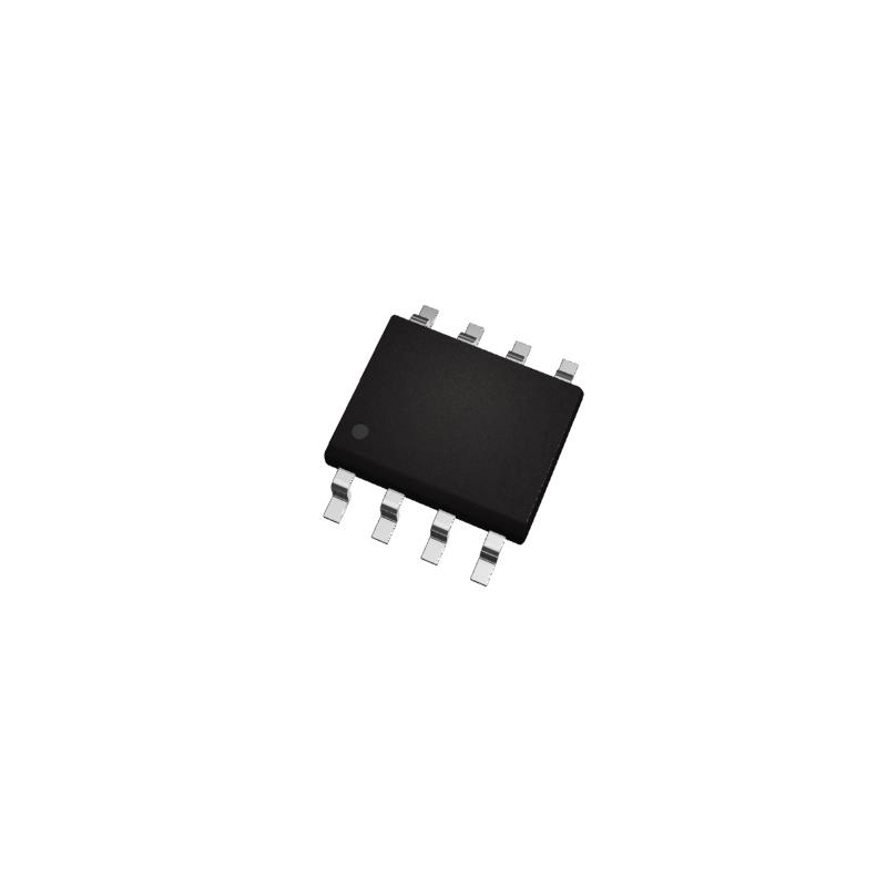
$5000MXIC MX25L512MC-12G
High-capacity, low-voltage NOR Flash chip for efficient data storage and retrieval


Marcas: MXIC
Parte do fabricante #: MX25L512MC-12G
Ficha de dados: MX25L512MC-12G Ficha de dados (PDF)
Pacote/Caso: SOP-8
Tipo de Produto: Microcontrollers
Status RoHS:
Condição de estoque: 5.290 peças, novo original
Warranty: 1 Year Ovaga Warranty - Find Out More
0
1
MX25L512MC-12G Descrição geral
GENERAL DESCRIPTION MX25L1005 is a CMOS 1,048,576 bit serial Flash memory, which is configured as 131,072 x 8 internally.The MX25L1005 feature a serial peripheral interface and software protocol allowing operation on a simple 3-wire bus. The three bus signals are a clock input (SCLK), a serial data input (SI), and a serial data output (SO). SPI access to the device is enabled by CS# input. The MX25L1005 provide sequential read operation on whole chip. After program/erase command is issued, auto program/ erase algorithms which program/ erase and verify the specified page or sector/block locations will be executed. Program command is executed on page (256 bytes) basis, and erase command is executes on chip or sector(4K-bytes) or block(64K-bytes). To provide user with ease of interface, a status register is included to indicate the status of the chip. The status read command can be issued to detect completion status of a program or erase operation via WIP bit. When the device is not in operation and CS# is high, it is put in standby mode and draws less than 10uA DC current. The MX25L1005 utilize MXIC's proprietary memory cell, which reliably stores memory contents even after 100,000 program and erase cycles.FEATURES GENERAL • Serial Peripheral Interface (SPI) compatible -- Mode 0 and Mode 3 • 1,048,576 x 1 bit structure • 32 Equal Sectors with 4K byte each - Any Sector can be erased individually • 2 Equal Blocks with 64K byte each - Any Block can be erased individually • Single Power Supply Operation - 2.7 to 3.6 volt for read, erase, and program operations • Latch-up protected to 100mA from -1V to Vcc +1V • Low Vcc write inhibit is from 1.5V to 2.5VPERFORMANCE • High Performance - Fast access time: 85MHz serial clock (15pF + 1TTL Load) and 66MHz serial clock (30pF + 1TTL Load) - Fast program time: 1.4ms(typ.) and 5ms(max.)/page (256-byte per page) - Fast erase time: 60ms(typ.) and 120ms(max.)/sector (4K-byte per sector) ; 1s(typ.) and 2s(max.)/block (64K-byte per block) • Low Power Consumption - Low active read current: 12mA(max.) at 85MHz, 8mA(max.) at 66MHz and 4mA(max.) at 33MHz - Low active programming current: 15mA (max.) - Low active erase current: 15mA (max.) - Low standby current: 10uA (max.) - Deep power-down mode 1uA (typical) • Minimum 100,000 erase/program cyclesSOFTWARE FEATURES • Input Data Format - 1-byte Command code • Block Lock protection - The BP0~BP1 status bit defines the size of the area to be software protected against Program and Erase instructions. • Auto Erase and Auto Program Algorithm - Automatically erases and verifies data at selected sector - Automatically programs and verifies data at selected page by an internal algorithm that automatically times the program pulse widths (Any page to be programed should have page in the erased state first) • Status Register Feature • Electronic Identification - JEDEC 2-byte Device ID - RES command, 1-byte Device IDHARDWARE FEATURES • SCLK Input - Serial clock input • SI Input - Serial Data Input • SO Output - Serial Data Output • WP# pin - Hardware write protection • HOLD# pin - pause the chip without diselecting the chip • PACKAGE - 8-pin SOP (150mil) - 8-land USON (2x3x0.6mm)* - All Pb-free devices are RoHS Compliant
Características
- GENERAL
- Serial Peripheral Interface (SPI) compatible -- Mode 0 and Mode 3
- 1,048,576 x 1 bit structure
- 32 Equal Sectors with 4K byte each
- - Any Sector can be erased individually
- 2 Equal Blocks with 64K byte each
- - Any Block can be erased individually
- Single Power Supply Operation
- - 2.7 to 3.6 volt for read, erase, and program operations
- Latch-up protected to 100mA from -1V to Vcc +1V
- Low Vcc write inhibit is from 1.5V to 2.5V
- PERFORMANCE
- High Performance
- - Fast access time: 85MHz serial clock (15pF + 1TTL Load) and 66MHz serial clock (30pF + 1TTL Load)
- - Fast program time: 1.4ms(typ.) and 5ms(max.)/page (256-byte per page)
- - Fast erase time: 60ms(typ.) and 120ms(max.)/sector (4K-byte per sector) ; 1s(typ.) and 2s(max.)/block (64K-byte per block)
- Low Power Consumption
- - Low active read current: 12mA(max.) at 85MHz, 8mA(max.) at 66MHz and 4mA(max.) at 33MHz
- - Low active programming current: 15mA (max.)
- - Low active erase current: 15mA (max.)
- - Low standby current: 10uA (max.)
- - Deep power-down mode 1uA (typical)
- Minimum 100,000 erase/program cycles
- SOFTWARE FEATURES
- Input Data Format
- - 1-byte Command code
- Block Lock protection
- - The BP0~BP1 status bit defines the size of the area to be software protected against Program and Erase instructions.
- Auto Erase and Auto Program Algorithm
- - Automatically erases and verifies data at selected sector
- - Automatically programs and verifies data at selected page by an internal algorithm that automatically times the program pulse widths (Any page to be programed should have page in the erased state first)
- Status Register Feature
- Electronic Identification
- - JEDEC 2-byte Device ID
- - RES command, 1-byte Device ID
- HARDWARE FEATURES
- SCLK Input
- - Serial clock input
- SI Input
- - Serial Data Input
- SO Output
- - Serial Data Output
- WP# pin
- - Hardware write protection
- HOLD# pin
- - pause the chip without diselecting the chip
- PACKAGE
- - 8-pin SOP (150mil)
- - 8-land USON (2x3x0.6mm)
- - All Pb-free devices are RoHS Compliant

Especificações
| Parâmetro | Valor | Parâmetro | Valor |
|---|---|---|---|
| Manufacturer | Macronix |
Envio
| Tipo de envio | Taxa de envio | Tempo de espera | |
|---|---|---|---|
 |
DHL | $20.00-$40.00 (0.50 KG) | 2-5 dias |
 |
FedEx | $20.00-$40.00 (0.50 KG) | 2-5 dias |
 |
UPS | $20.00-$40.00 (0.50 KG) | 2-5 dias |
 |
TNT | $20.00-$40.00 (0.50 KG) | 2-5 dias |
 |
EMS | $20.00-$40.00 (0.50 KG) | 2-5 dias |
 |
CORREIO AÉREO REGISTADO | $20.00-$40.00 (0.50 KG) | 2-5 dias |
Tempo de processamento: A taxa de envio depende de diferentes zonas e países.
Pagamento
| Termos de pagamento | Taxa de mão | |
|---|---|---|
 |
Transferência bancária | cobrar taxa bancária de US$ 30,00. |
 |
PayPal | cobrar taxa de serviço de 4,0%. |
 |
Cartão de crédito | cobrar taxa de serviço de 3,5%. |
 |
Western Union | charge US.00 banking fee. |
 |
Grama de dinheiro | cobrar taxa bancária de US$ 0,00. |
Garantias
1.Os componentes eletrônicos que você compra incluem garantia de 365 dias, garantimos a qualidade do produto.
2. se alguns dos itens que você recebeu não forem de qualidade perfeita, providenciaremos seu reembolso ou substituição com responsabilidade. Mas os itens devem permanecer em sua condição original.
Embalagem
-

Etapa1 :produtos
-

Etapa2 :Embalagem a vácuo
-

Etapa3 :Saco antiestático
-

Etapa4 :Embalagem individual
-

Etapa5 :Caixas de embalagem
-

Etapa6 :etiqueta de envio com código de barras


Todos os produtos serão embalados em saco antiestático. Envio com proteção antiestática ESD.
Fora da etiqueta da embalagem ESD serão utilizadas as informações da nossa empresa: Número da peça, marca e quantidade.
Iremos inspecionar todas as mercadorias antes do envio, garantir que todos os produtos estejam em boas condições e garantir que as peças sejam novas folhas de dados originais.
Depois que todas as mercadorias forem garantidas sem problemas na pós-embalagem, embalaremos com segurança e enviaremos por expresso global. Apresenta excelente resistência a perfurações e rasgos, além de boa integridade de vedação.


Oferecemos produtos de alta qualidade, serviço atencioso e garantia pós-venda
-

Temos produtos ricos que podem atender às suas diversas necessidades.
-

A quantidade mínima de pedido começa em 1 unidade.
-

A menor taxa de envio internacional começa em US$ 0,00
-

365 dias de garantia de qualidade para todos os produtos