

As imagens são apenas para referência. Consulte as especificações do produto
Pedidos acima de
$5000LCMXO3LF-1300C-5BG256I
This FPGA operates at a voltage of 1.2V and comes in a 256-pin chip-scale package (CABGA) configuration, delivered in a tray format


Marcas: Lattice Semiconductor Corporation
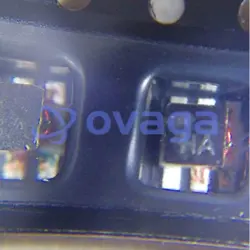
Parte do fabricante #: LCMXO3LF-1300C-5BG256I
Ficha de dados: LCMXO3LF-1300C-5BG256I Ficha de dados (PDF)
Pacote/Caso: 256-LFBGA
Tipo de Produto: FPGAs (Field Programmable Gate Array)
Status RoHS:
Condição de estoque: 8.745 peças, novo original
Warranty: 1 Year Ovaga Warranty - Find Out More
0
1
LCMXO3LF-1300C-5BG256I Descrição geral
The LCMXO3LF-1300C-5BG256I FPGA, manufactured by Lattice Semiconductor, offers a compelling combination of performance and energy efficiency. With a logic cell count of 1300 and a maximum speed grade of 5, this low-cost, low-power FPGA is capable of handling small to medium-sized designs with ease. Its 256-pin BGA package ensures a compact form factor, making it a great fit for space-constrained applications, while its low power consumption makes it ideal for mobile devices, IoT applications, and other battery-powered devices. Additionally, the LCMXO3LF-1300C-5BG256I boasts embedded block RAM, DSP blocks, and flexible I/O options, allowing for versatile and efficient design implementations across a wide range of applications
Características
- Non-volatile, Infinitely Reconfigurable
- Instant-on – powers up in microseconds
- Single chip, no external configuration memory
- required
- Excellent design security, no bit stream to
- intercept
- Reconfigure SRAM based logic in milliseconds
- SRAM and non-volatile memory programmable
- through JTAG port
- Supports background programming of
- non-volatile memory
- Sleep Mode
- Allows up to 100x static current reduction
- TransFR™ Reconfiguration (TFR)
- In-field logic update while system operates
- High I/O to Logic Density
- 256 to 2280 LUT4s
- 73 to 271 I/Os with extensive package options
- Density migration supported
- Lead free/RoHS compliant packaging
- Embedded and Distributed Memory
- Up to 27.6 Kbits sysMEM™ Embedded Block
- Up to 7.5 Kbits distributed RAM
- Dedicated FIFO control logic
- Flexible I/O Buffer
- Programmable sysIO™ buffer supports wide
- range of interfaces:
- − LVCMOS 3.3/2.5/1.8/1.5/1.2
- − LVTTL
- − LVDS, Bus-LVDS, LVPECL, RSDS
- sysCLOCK™ PLLs
- Up to two analog PLLs per device
- Clock multiply, divide, and phase shifting
- System Level Support
- IEEE Standard 1149.1 Boundary Scan
- Onboard oscillator
- Devices operate with 3.3V, 2.5V, 1.8V or 1.2V
- power supply
- IEEE 1532 compliant in-system programming
Especificações
| Parâmetro | Valor | Parâmetro | Valor |
|---|---|---|---|
| Series | MachXO3 | Package | Tray |
| Product Status | Active | Programmabe | Not Verified |
| Number of LABs/CLBs | 160 | Number of Logic Elements/Cells | 1280 |
| Total RAM Bits | 65536 | Number of I/O | 206 |
| Voltage - Supply | 2.375V ~ 3.465V | Mounting Type | Surface Mount |
| Operating Temperature | -40°C ~ 100°C (TJ) | Package / Case | 256-LFBGA |
| Supplier Device Package | 256-CABGA (14x14) |
Envio
| Tipo de envio | Taxa de envio | Tempo de espera | |
|---|---|---|---|
 |
DHL | $20.00-$40.00 (0.50 KG) | 2-5 dias |
 |
FedEx | $20.00-$40.00 (0.50 KG) | 2-5 dias |
 |
UPS | $20.00-$40.00 (0.50 KG) | 2-5 dias |
 |
TNT | $20.00-$40.00 (0.50 KG) | 2-5 dias |
 |
EMS | $20.00-$40.00 (0.50 KG) | 2-5 dias |
 |
CORREIO AÉREO REGISTADO | $20.00-$40.00 (0.50 KG) | 2-5 dias |
Tempo de processamento: A taxa de envio depende de diferentes zonas e países.
Pagamento
| Termos de pagamento | Taxa de mão | |
|---|---|---|
 |
Transferência bancária | cobrar taxa bancária de US$ 30,00. |
 |
PayPal | cobrar taxa de serviço de 4,0%. |
 |
Cartão de crédito | cobrar taxa de serviço de 3,5%. |
 |
Western Union | charge US.00 banking fee. |
 |
Grama de dinheiro | cobrar taxa bancária de US$ 0,00. |
Garantias
1.Os componentes eletrônicos que você compra incluem garantia de 365 dias, garantimos a qualidade do produto.
2. se alguns dos itens que você recebeu não forem de qualidade perfeita, providenciaremos seu reembolso ou substituição com responsabilidade. Mas os itens devem permanecer em sua condição original.
Embalagem
-

Etapa1 :produtos
-

Etapa2 :Embalagem a vácuo
-

Etapa3 :Saco antiestático
-

Etapa4 :Embalagem individual
-

Etapa5 :Caixas de embalagem
-

Etapa6 :etiqueta de envio com código de barras


Todos os produtos serão embalados em saco antiestático. Envio com proteção antiestática ESD.
Fora da etiqueta da embalagem ESD serão utilizadas as informações da nossa empresa: Número da peça, marca e quantidade.
Iremos inspecionar todas as mercadorias antes do envio, garantir que todos os produtos estejam em boas condições e garantir que as peças sejam novas folhas de dados originais.
Depois que todas as mercadorias forem garantidas sem problemas na pós-embalagem, embalaremos com segurança e enviaremos por expresso global. Apresenta excelente resistência a perfurações e rasgos, além de boa integridade de vedação.


Part points
-
The LCMXO3LF-1300C-5BG256I chip is a low-power, small-footprint FPGA (field-programmable gate array) from Lattice Semiconductor. It features 1300 LUTs, 317 Kbits of embedded memory, and 36 I/Os. This chip is ideal for applications requiring low power consumption and space constraints.
-
Equivalent
The equivalent products of the LCMXO3LF-1300C-5BG256I chip are the LCMXO3 series from Lattice Semiconductor, including the LCMXO3LF-1300C-6BG256I and the LCMXO3LF-1300C-6BG324I. These chips offer similar features and functionality, providing alternative options for design and integration. -
Features
LCMXO3LF-1300C-5BG256I features 1300 LUTs, 640 macrocells, 6 kilobits of RAM, 32 I/Os, and is housed in a 256-ball grid array package. It has low power consumption, small form factor, and is ideal for low power applications in industrial, consumer, and automotive markets. -
Pinout
The LCMXO3LF-1300C-5BG256I is a low-power FPGA with 256 pins. It is designed for use in low-power applications and features 1300 LUTs. It also includes 4 Multiplier/Accumulators and 32 I/O pins. -
Manufacturer
LCMXO3LF-1300C-5BG256I is manufactured by Lattice Semiconductor Corporation, a company specializing in low-power, small form-factor programmable logic devices. Lattice Semiconductor Corporation is a leading provider of smart connectivity solutions, offering customizable solutions for a wide range of applications in consumer, automotive, industrial, and communications markets. -
Application Field
The LCMXO3LF-1300C-5BG256I can be used in a variety of application areas such as battery management systems, sensor interfaces, portable medical devices, and industrial automation. Its low power consumption, small form factor, and high integration make it ideal for applications requiring low power consumption and high performance in a compact package. -
Package
The LCMXO3LF-1300C-5BG256I chip is in a 256-ball Fine-pitch Ball Grid Array (FPBGA) package. It is a Field-Programmable Gate Array (FPGA) in a form of a chip. The size of the chip is 13mm x 13mm.


Oferecemos produtos de alta qualidade, serviço atencioso e garantia pós-venda
-

Temos produtos ricos que podem atender às suas diversas necessidades.
-

A quantidade mínima de pedido começa em 1 unidade.
-

A menor taxa de envio internacional começa em US$ 0,00
-

365 dias de garantia de qualidade para todos os produtos