

As imagens são apenas para referência. Consulte as especificações do produto
Pedidos acima de
$5000
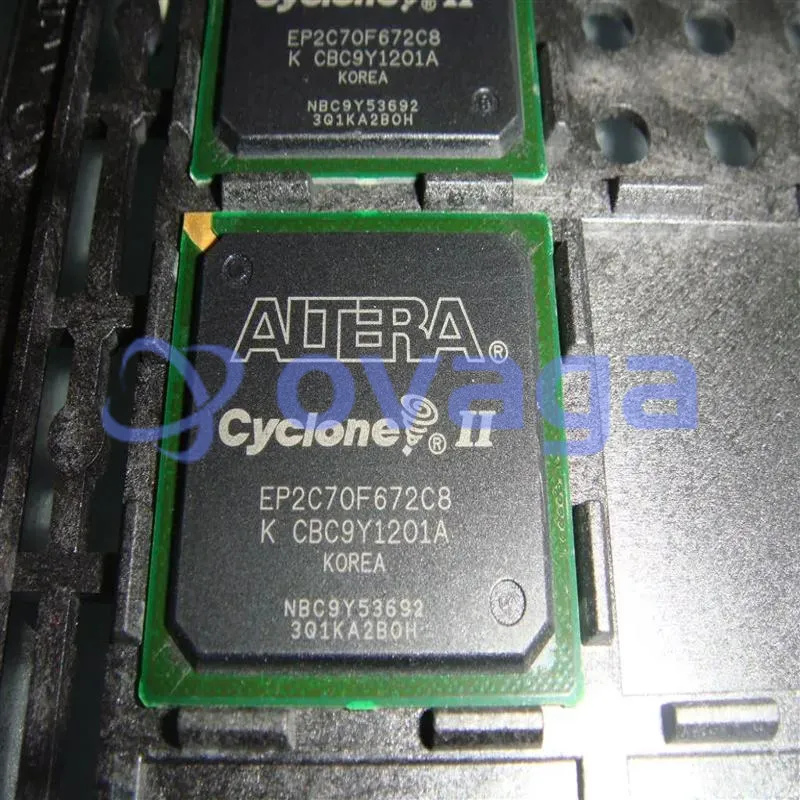
Intel EP2C70F672C8

ROHS Compliant EP2C70F672C8 68416 4276 FBGA-672(27x27) Programmable Logic Device


Marcas: INTEL CORP
Parte do fabricante #: EP2C70F672C8
Ficha de dados: EP2C70F672C8 Ficha de dados (PDF)
Pacote/Caso: FBGA-672
Status RoHS:
Condição de estoque: 6.554 peças, novo original
Tipo de Produto: FPGAs (Field Programmable Gate Array)
Warranty: 1 Year Ovaga Warranty - Find Out More
0
1
*Todos os preços estão em USD
| Quantidade | Preço unitário | Preço Externo |
|---|---|---|
| 1 | $1408,287 | $1408,287 |
| 200 | $561,916 | $112383,200 |
| 480 | $543,139 | $260706,720 |
| 1000 | $533,860 | $533860,000 |
Em estoque: 6.554 PCS
EP2C70F672C8 Descrição geral
In conclusion, the EP2C70F672C8 FPGA from Intel (formerly Altera) stands as a reliable and efficient solution for complex digital designs. With its high logic element count, embedded memory, dedicated multipliers, and various I/O options, this FPGA is well-suited for a wide range of applications in telecommunications, automotive, industrial control, and more. Its support for Intel's Quartus Prime development software further enhances its usability, making it a valuable tool for engineers and designers working on advanced projects
Características
- High-density architecture with 4,608 to 68,416 LEs
- M4K embedded memory blocks
- Up to 1.1 Mbits of RAM available without reducing available logic
- 4,096 memory bits per block (4,608 bits per block including 512 parity bits)
- Variable port configurations of ×1, ×2, ×4, ×8, ×9, ×16, ×18, ×32, and ×36
- True dual-port (one read and one write, two reads, or two writes) operation for ×1, ×2, ×4, ×8, ×9, ×16, and ×18 modes
- Byte enables for data input masking during writes
- Up to 260-MHz operation
- Embedded multipliers
- Up to 150 18- × 18-bit multipliers are each configurable as two independent 9- × 9-bit multipliers with up to 250-MHz performance
- Optional input and output registers
- Advanced I/O support
- High-speed differential I/O standard support, including LVDS, RSDS, mini-LVDS, LVPECL, differential HSTL, and differential SSTL
- Single-ended I/O standard support, including 2.5-V and 1.8-V, SSTL class I and II, 1.8-V and 1.5-V HSTL class I and II, 3.3-V PCI and PCI-X 1.0, 3.3-, 2.5-, 1.8-, and 1.5-V LVCMOS, and 3.3-, 2.5-, and 1.8-V LVTTL
- Peripheral Component Interconnect Special Interest Group (PCI SIG) PCI Local Bus Specification, Revision 3.0 compliance for 3.3-V operation at 33 or 66 MHz for 32- or 64-bit interfaces
- PCI Express with an external TI PHY and an Altera PCI Express ×1 Megacore® function
- 133-MHz PCI-X 1.0 specification compatibility
- High-speed external memory support, including DDR, DDR2, and SDR SDRAM, and QDRII SRAM supported by drop in Altera IP MegaCore functions for ease of use
- Three dedicated registers per I/O element (IOE): one input register, one output register, and one output-enable register
- Programmable bus-hold feature
- Programmable output drive strength feature
- Programmable delays from the pin to the IOE or logic array
- I/O bank grouping for unique VCCIO and/or VREF bank settings
- MultiVolt™ I/O standard support for 1.5-, 1.8-, 2.5-, and 3.3-interfaces
- Hot-socketing operation support
- Tri-state with weak pull-up on I/O pins before and during configuration
- Programmable open-drain outputs
- Series on-chip termination support
- (Continue .)

Especificações
| Parâmetro | Valor | Parâmetro | Valor |
|---|---|---|---|
| Rohs Code | No | Part Life Cycle Code | Active |
| Ihs Manufacturer | INTEL CORP | Package Description | FBGA-672 |
| Reach Compliance Code | compliant | HTS Code | 8542.39.00.01 |
| Additional Feature | ALSO REQUIRES 3.3 SUPPLY | Clock Frequency-Max | 402.5 MHz |
| JESD-30 Code | S-PBGA-B672 | JESD-609 Code | e0 |
| Length | 27 mm | Moisture Sensitivity Level | 3 |
| Number of CLBs | 4276 | Number of Inputs | 422 |
| Number of Logic Cells | 68416 | Number of Outputs | 406 |
| Number of Terminals | 672 | Operating Temperature-Max | 85 °C |
| Operating Temperature-Min | Organization | 4276 CLBS | |
| Package Body Material | PLASTIC/EPOXY | Package Code | BGA |
| Package Equivalence Code | BGA672,26X26,40 | Package Shape | SQUARE |
| Package Style | GRID ARRAY | Power Supplies | 1.2,1.5/3.3,3.3 V |
| Programmable Logic Type | FIELD PROGRAMMABLE GATE ARRAY | Qualification Status | Not Qualified |
| Seated Height-Max | 2.6 mm | Supply Voltage-Max | 1.25 V |
| Supply Voltage-Min | 1.15 V | Supply Voltage-Nom | 1.2 V |
| Surface Mount | YES | Technology | CMOS |
| Temperature Grade | OTHER | Terminal Finish | TIN LEAD |
| Terminal Form | BALL | Terminal Pitch | 1 mm |
| Terminal Position | BOTTOM |
Envio
| Tipo de envio | Taxa de envio | Tempo de espera | |
|---|---|---|---|
 |
DHL | $20.00-$40.00 (0.50 KG) | 2-5 dias |
 |
FedEx | $20.00-$40.00 (0.50 KG) | 2-5 dias |
 |
UPS | $20.00-$40.00 (0.50 KG) | 2-5 dias |
 |
TNT | $20.00-$40.00 (0.50 KG) | 2-5 dias |
 |
EMS | $20.00-$40.00 (0.50 KG) | 2-5 dias |
 |
CORREIO AÉREO REGISTADO | $20.00-$40.00 (0.50 KG) | 2-5 dias |
Tempo de processamento: A taxa de envio depende de diferentes zonas e países.
Pagamento
| Termos de pagamento | Taxa de mão | |
|---|---|---|
 |
Transferência bancária | cobrar taxa bancária de US$ 30,00. |
 |
PayPal | cobrar taxa de serviço de 4,0%. |
 |
Cartão de crédito | cobrar taxa de serviço de 3,5%. |
 |
Western Union | charge US.00 banking fee. |
 |
Grama de dinheiro | cobrar taxa bancária de US$ 0,00. |
Garantias
1.Os componentes eletrônicos que você compra incluem garantia de 365 dias, garantimos a qualidade do produto.
2. se alguns dos itens que você recebeu não forem de qualidade perfeita, providenciaremos seu reembolso ou substituição com responsabilidade. Mas os itens devem permanecer em sua condição original.
Embalagem
-

Etapa1 :produtos
-

Etapa2 :Embalagem a vácuo
-

Etapa3 :Saco antiestático
-

Etapa4 :Embalagem individual
-

Etapa5 :Caixas de embalagem
-

Etapa6 :etiqueta de envio com código de barras


Todos os produtos serão embalados em saco antiestático. Envio com proteção antiestática ESD.
Fora da etiqueta da embalagem ESD serão utilizadas as informações da nossa empresa: Número da peça, marca e quantidade.
Iremos inspecionar todas as mercadorias antes do envio, garantir que todos os produtos estejam em boas condições e garantir que as peças sejam novas folhas de dados originais.
Depois que todas as mercadorias forem garantidas sem problemas na pós-embalagem, embalaremos com segurança e enviaremos por expresso global. Apresenta excelente resistência a perfurações e rasgos, além de boa integridade de vedação.


Part points
-
The EP2C70F672C8 is a field-programmable gate array (FPGA) chip manufactured by Intel. It belongs to the Cyclone II family and features 70,000 logic elements, 622 user I/O pins, and 504 embedded multipliers. With its configurable nature, it's widely used in various applications such as telecommunications, industrial automation, and consumer electronics.
-
Equivalent
The EP2C70F672C8 chip is part of Altera's Cyclone II FPGA series. Equivalent products include Xilinx's Spartan-3, Lattice Semiconductor's MachXO2, and Microchip's SmartFusion2. Each offers similar programmable logic capabilities, though specifics may vary. -
Features
The EP2C70F672C8 is an Altera Cyclone II FPGA. Its features include 70,000 logic elements, 4 Mbits of embedded memory, 266 MHz maximum core frequency, and 672 user I/O pins. It operates on a 1.2V core voltage and supports various communication protocols like PCIe and Gigabit Ethernet. -
Pinout
The EP2C70F672C8 is an FPGA with 672 pins. Its functions include programmable logic, configurable I/Os, memory blocks, and DSP slices for flexible customization and high-performance computing tasks. -
Manufacturer
The EP2C70F672C8 is manufactured by Altera Corporation, now part of Intel Corporation. Altera specialized in manufacturing programmable logic devices, particularly field-programmable gate arrays (FPGAs). FPGAs are integrated circuits designed to be configured by a customer or a designer after manufacturing, allowing for customizable hardware solutions in various applications like telecommunications, automotive, and industrial automation. -
Application Field
The EP2C70F672C8 is commonly used in a variety of applications, including telecommunications, industrial automation, automotive, and aerospace. It is suitable for applications that require high-performance processing, reliable operation, and low power consumption. Its FPGA architecture allows for flexibility and adaptability in a range of different environments. -
Package
The EP2C70F672C8 chip is a Field-Programmable Gate Array (FPGA) from Intel (formerly Altera). It comes in a Ball Grid Array (BGA) package with a form factor of 672-pin. The package size is 27mm x 27mm.


Oferecemos produtos de alta qualidade, serviço atencioso e garantia pós-venda
-

Temos produtos ricos que podem atender às suas diversas necessidades.
-

A quantidade mínima de pedido começa em 1 unidade.
-

A menor taxa de envio internacional começa em US$ 0,00
-

365 dias de garantia de qualidade para todos os produtos


