

As imagens são apenas para referência. Consulte as especificações do produto
Pedidos acima de
$5000ADI ADSP-2191
DSPMicrocomputer


Marcas: ADI
Parte do fabricante #: ADSP-2191
Ficha de dados: ADSP-2191 Ficha de dados (PDF)
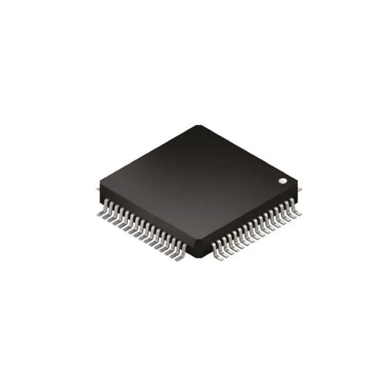
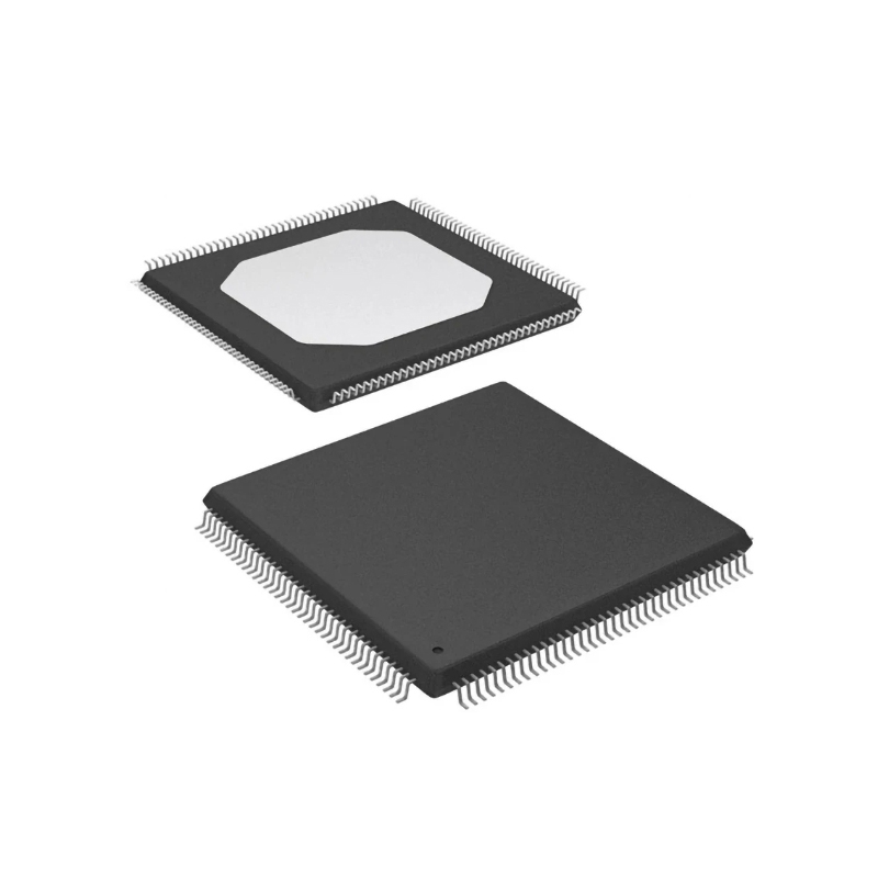
Pacote/Caso: BGA
Status RoHS:
Condição de estoque: 6.554 peças, novo original
Warranty: 1 Year Ovaga Warranty - Find Out More
0
1
ADSP-2191 Descrição geral
GENERAL DESCRIPTIONThe ADSP-2191M DSP is a single-chip microcomputer optimized for digital signal processing (DSP) and other high speed numeric processing applications.The ADSP-2191M combines the ADSP-219x family base architecture (three computational units, two data address gener ators, and a program sequencer) with three serial ports, two SPI-compatible ports, one UART port, a DMA controller, three programmable timers, general-purpose Programmable Flag pins, extensive interrupt capabilities, and on-chip program and data memory spaces.The ADSP-2191M architecture is code-compatible with DSPs of the ADSP-218x family. Although the architectures are compatible, the ADSP-2191M architecture has a number of enhancements over the ADSP-218x architecture. The enhance ments to computational units, data address generators, and program sequencer make the ADSP-2191M more flexible and even easier to program.PERFORMANCE FEATURES 6.25 ns Instruction Cycle Time, for up to 160 MIPS Sustained Performance ADSP-218x Family Code Compatible with the Same Easy to Use Algebraic Syntax Single-Cycle Instruction Execution Single-Cycle Context Switch between Two Sets of Computation and Memory Instructions Instruction Cache Allows Dual Operand Fetches in Every Instruction Cycle Multifunction Instructions Pipelined Architecture Supports Efficient Code Execution Architectural Enhancements for Compiled C and C++ Code Efficiency Architectural Enhancements beyond ADSP-218x Family are Supported with Instruction Set Extensions for Added Registers, and Peripherals Flexible Power Management with User-Selectable Power-Down and Idle ModesINTEGRATION FEATURES 160 K Bytes On-Chip RAM Configured as 32K Words 24-Bit Memory RAM and 32K Words 16-Bit Memory RAM Dual-Purpose 24-Bit Memory for Both Instruction and Data Storage Independent ALU, Multiplier/Accumulator, and Barrel Shifter Computational Units with Dual 40-bit Accumulators Unified Memory Space Allows Flexible Address Generation, Using Two Independent DAG Units Powerful Program Sequencer Provides Zero-Overhead Looping and Conditional Instruction Execution Enhanced Interrupt Controller Enables Programming of Interrupt Priorities and Nesting ModesSYSTEM INTERFACE FEATURES Host Port with DMA Capability for Glueless 8- or 16-Bit Host Interface 16-Bit External Memory Interface for up to 16M Words of Addressable Memory Space Three Full-Duplex Multichannel Serial Ports, with Support for H.100 and up to 128 TDM Channels with A-Law and μ-Law Companding Optimized for Telecom munications Systems Two SPI-Compatible Ports with DMA Support UART Port with DMA Support 16 General-Purpose I/O Pins with Integrated Interrupt Support Three Programmable Interval Timers with PWM Generation, PWM Capture/Pulsewidth Measurement, and External Event Counter Capabilities Up to 11 DMA Channels Can Be Active at Any Given Time for High I/O Throughput On-Chip Boot ROM for Automatic Booting from External 8- or 16-Bit Host Device, SPI ROM, or UART with Autobaud Detection Programmable PLL Supports 1x to 32x Input Frequency Multiplication and Can Be Altered during Runtime IEEE JTAG Standard 1149.1 Test Access Port Supports On-Chip Emulation and System Debugging 2.5 V Internal Operation and 3.3 V I/O 144-Lead LQFP and 144-Ball Mini-BGA Packages
Características
- 6.25 ns Instruction Cycle Time (Internal), for up to
- 160 MIPS Sustained Performance
- ADSP-218x Family Code Compatible with the Same
- Easy -to-Use Algebraic Syntax
- Single-Cycle Instruction Execution
- Up to 16M words of Addressable Memory Space with
- 24 Bits of Addressing Width
- Dual Purpose Program Memory for Both Instruction and
- Data Storage
- Fully Transparent Instruction Cache Allows Dual
- Operand Fetches in Every Instruction Cycle
- Unified Memory Space Permits Flexible Address
- Generation, Using Two Independent DAG Units
- Independent ALU, Multiplier/Accumulator, and Barrel
- Shifter Computational Units with Dual 40-bit Accumulators
- Single-Cycle Context Switch between Two Sets of Computational and DAG Registers
- Parallel Execution of Computation and Memory Instructions
- Pipelined Architecture Supports Efficient Code
- Execution at Speeds up to 160 MIPS
- Register File Computations with All Nonconditional,
- Nonparallel Computational Instructions
- Powerful Program Sequencer Provides Zero-Overhead
- Looping and Conditional Instruction Execution
- Architectural Enhancements for Compiled C Code Efficiency
- ADSP-2191 DSP FEATURES
- 64K Words of On-Chip RAM, Configured as 32K Words
- On-Chip 24-bit RAM and 32K Words On-Chip
- 16-bit RAM
- Architecture Enhancements beyond ADSP-218x Family
- are Supported with Instruction Set Extensions for
- Added Registers, Ports, and Peripherals
- Flexible Power Management with Selectable
- Power-Down and Idle Modes
- Programmable PLL Supports 1x to 32x Frequency
- Multiplication, Enabling Full-Speed Operation from
- Low-Speed Input Clocks
- 2.5 V Internal Operation Supports 3.3 V Compliant I/O
- Three Full-Duplex Multichannel Serial Ports, Each
- Supporting H.100 Standard with A-Law and μ-Law
- Companding in Hardware
- Two SPI-Compatible Ports with DMA Capability
- One UART Port with DMA Capability
- 16 General-Purpose I/O Pins (Eight Dedicated/Eight
- Programmable from the External Memory Interface)
- with Integrated Interrupt Support
- Three Programmable 32-Bit Interval Timers with
- Pulsewidth Counter, PWM Generation, and Externally
- Clocked Timer Capabilities
- Up to 11 DMA Channels can be Active at any Given Time
- Host Port With DMA Capability for Efficient, Glueless Host
- Interface (16-Bit Transfers)
- External Memory Interface Features Include:
- Direct Access from the DSP to External Memory for
- Data and Instructions.
- Support for DMA Block Transfers to/from
- External Memory.
- Separate Peripheral Memory Space with Parallel
- Support for 224K External 16-Bit Registers.
- Four General-Purpose Memory Select Signals that
- Provide Access to Separate Banks of External
- Memory. Bank Boundaries and Size Are User
- Programmable.
- Programmable Waitstate Logic with ACK Signal and
- Separate Read and Write Wait Counts. Wait Mode
- Completion Supports All Combinations of ACK
- and/or Wait Count.
- I/O Clock Rate Can Be Set to the Peripheral Clock Rate
- Divided by 1, 2, 4, 16, or 32 to Allow Interface to Slow
- Memory Devices.
- Address Translation and Data Word Packing is Provided
- to Support an 8- or 16-Bit External Data Bus.
- Programmable Read and Write Strobe Polarity.
- Separate Configuration Registers for the Four
- General-Purpose, Peripheral, and Boot
- Memory Spaces.
- Bus Request and Grant Signals Support the Use of the
- External Bus by an External Device.
- Boot Methods Include Booting Through External Memory
- Interface, SPI Ports, UART Port, or Host Interface
- IEEE JTAG Standard 1149.1 Test Access Port Supports
- On-Chip Emulation and System Debugging
- 144-Lead LQFP Package (20 x 20 x 1.4 mm) and 144-Lead
- Mini-BGA Package (10 x 10 x 1.25 mm)
Envio
| Tipo de envio | Taxa de envio | Tempo de espera | |
|---|---|---|---|
 |
DHL | $20.00-$40.00 (0.50 KG) | 2-5 dias |
 |
FedEx | $20.00-$40.00 (0.50 KG) | 2-5 dias |
 |
UPS | $20.00-$40.00 (0.50 KG) | 2-5 dias |
 |
TNT | $20.00-$40.00 (0.50 KG) | 2-5 dias |
 |
EMS | $20.00-$40.00 (0.50 KG) | 2-5 dias |
 |
CORREIO AÉREO REGISTADO | $20.00-$40.00 (0.50 KG) | 2-5 dias |
Tempo de processamento: A taxa de envio depende de diferentes zonas e países.
Pagamento
| Termos de pagamento | Taxa de mão | |
|---|---|---|
 |
Transferência bancária | cobrar taxa bancária de US$ 30,00. |
 |
PayPal | cobrar taxa de serviço de 4,0%. |
 |
Cartão de crédito | cobrar taxa de serviço de 3,5%. |
 |
Western Union | charge US.00 banking fee. |
 |
Grama de dinheiro | cobrar taxa bancária de US$ 0,00. |
Garantias
1.Os componentes eletrônicos que você compra incluem garantia de 365 dias, garantimos a qualidade do produto.
2. se alguns dos itens que você recebeu não forem de qualidade perfeita, providenciaremos seu reembolso ou substituição com responsabilidade. Mas os itens devem permanecer em sua condição original.
Embalagem
-

Etapa1 :produtos
-

Etapa2 :Embalagem a vácuo
-

Etapa3 :Saco antiestático
-

Etapa4 :Embalagem individual
-

Etapa5 :Caixas de embalagem
-

Etapa6 :etiqueta de envio com código de barras


Todos os produtos serão embalados em saco antiestático. Envio com proteção antiestática ESD.
Fora da etiqueta da embalagem ESD serão utilizadas as informações da nossa empresa: Número da peça, marca e quantidade.
Iremos inspecionar todas as mercadorias antes do envio, garantir que todos os produtos estejam em boas condições e garantir que as peças sejam novas folhas de dados originais.
Depois que todas as mercadorias forem garantidas sem problemas na pós-embalagem, embalaremos com segurança e enviaremos por expresso global. Apresenta excelente resistência a perfurações e rasgos, além de boa integridade de vedação.


Oferecemos produtos de alta qualidade, serviço atencioso e garantia pós-venda
-

Temos produtos ricos que podem atender às suas diversas necessidades.
-

A quantidade mínima de pedido começa em 1 unidade.
-

A menor taxa de envio internacional começa em US$ 0,00
-

365 dias de garantia de qualidade para todos os produtos