

As imagens são apenas para referência. Consulte as especificações do produto
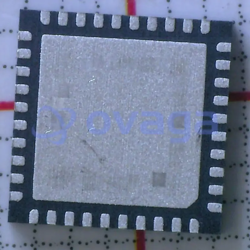
Renesas 8T49N241-998NLGI
Clock Generators & Support Products UFT 1 Integer 3 Frac 0.35ps EEProm 25MHz


Marcas: Renesas Technology Corp
Parte do fabricante #: 8T49N241-998NLGI
Ficha de dados: 8T49N241-998NLGI Datasheet (PDF)
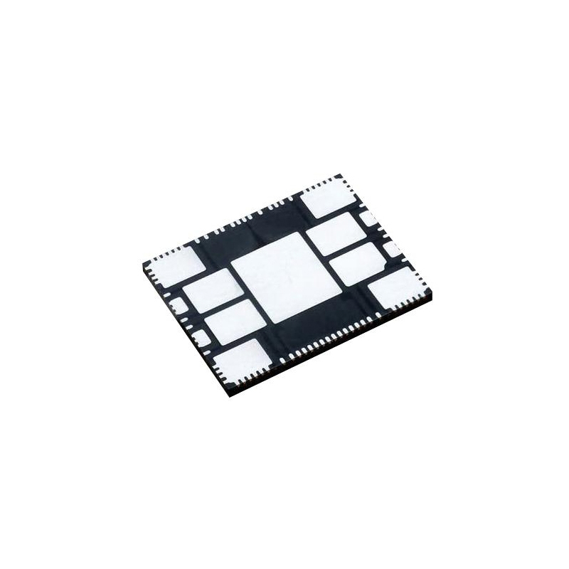
Pacote/Caso: VFQFPN-40
Tipo de Produto: Integrated Circuits (ICs)
Status RoHS:
Condição de estoque: 3047 peças, novo original
Warranty: 1 Year Ovaga Warranty - Find Out More
0
1
Adicionar à lista técnica8T49N241-998NLGI Descrição geral
The 8T49N241 has one fractional-feedback PLL that can be used as a frequency translator with jitter attenuation or a frequency synthesizer. It is equipped with one integer and three fractional output dividers, allowing the generation of up to four different and unrelated output frequencies, ranging from 8 kHz to 1 GHz. Output frequencies can be completely independent of the input frequencies, and all four of these frequencies can be completely independent of each other. The four outputs may select among LVPECL, LVDS, HCSL or LVCMOS output levels.
The 8T49N241 is ideal for use in a wide range of equipment, including 10G/40G/100G SONET/SDH and Ethernet network line cards, wireless base station baseband units, broadcast video, carrier Ethernet switches, OTN, or in test and measurement applications. For example, the 8T49N241 can be used in GbE/10GbE/100GbE Synchronous Ethernet line card applications in order to preserve the G.8262 compliance from the Synchronous Equipment Timing Source (SETS) on the timing card.
Renesas’ third generation Universal Frequency Translator family also includes the 8T49N242 (2-in / 1-PLL / 4-out), the 8T49N285 (2-in / 1-PLL / 8-out), the 8T49N286 (4-in / 2-PLL / 8-out) and the 8T49N287 (2-in / 2-PLL / 8-out). These devices are complemented by the 82P33714 and 82P33731 synchronous equipment timing source (SETS) for Synchronous Ethernet (SyncE) and 10G-40G SyncE, respectively.
To see other devices in this product family, visit the Universal Frequency Translators page.
Características
- Compliant with the requirements outlined in Telcordia GR-253-CORE (SONET) & ITU-T G.813/G.8262 (SDH/SONET & SyncE) when paired with a Synchronous Equipment Timing Source (SETS ) device
- Generates up to 4 LVPECL / LVDS/HCSL or 16 LVCMOS output clocks ranging from 8 kHz up to 1.0 GHz (diff), 8 kHz to 250 MHz (LVCMOS), that meet jitter limits for 10G up to 25G Ethernet applications
- 0.35ps RMS (including spurs), 12 kHz to 20 MHz
- Accepts up to two LVPECL, LVDS, LVHSTL, HCSL or LVCMOS input clocks ranging from 8 kHz up to 875 MHz
- Auto and manual input clock selection with hitless switching
- Clock input monitoring, including support for gapped clocks
- Phase-Slope Limiting and Fully Hitless Switching options to control output phase transients
- Operates from a 10 MHz to 50 MHz
- Register programmable through I2C or via external I2C EEPROM
- 8T49N241-998 “Boot from EEPROM”
- 8T49N241-999 “powers up disabled”
- Supported by Renesas Timing Commander Software™
Especificações
| Parâmetro | Valor | Parâmetro | Valor |
|---|---|---|---|
| Source Content uid | 8T49N241-998NLGI | Pbfree Code | Yes |
| Rohs Code | Yes | Part Life Cycle Code | Active |
| Ihs Manufacturer | RENESAS ELECTRONICS CORP | Part Package Code | VFQFPN |
| Package Description | VFQFPN-40 | Pin Count | 40 |
| Manufacturer Package Code | NLG40P2 | Reach Compliance Code | compliant |
| ECCN Code | NLR | HTS Code | 8542390001 |
| Samacsys Manufacturer | Renesas Electronics | Additional Feature | IT ALSO OPERATES AT 3.3V NOMINAL SUPPLY |
| JESD-30 Code | S-XQCC-N40 | Moisture Sensitivity Level | 3 |
| Number of Terminals | 40 | Package Body Material | UNSPECIFIED |
| Package Code | HVQCCN | Package Equivalence Code | LCC40,.24SQ,20 |
| Package Shape | SQUARE | Package Style | CHIP CARRIER, HEAT SINK/SLUG, VERY THIN PROFILE |
| Peak Reflow Temperature (Cel) | 260 | Surface Mount | YES |
| Technology | CMOS | Temperature Grade | INDUSTRIAL |
| Terminal Finish | TIN | Terminal Form | NO LEAD |
| Terminal Position | QUAD |
Envio
| Tipo de envio | Taxa de envio | Tempo de espera | |
|---|---|---|---|
 |
DHL | $20.00-$40.00 (0.50 KG) | 2-5 dias |
 |
FedEx | $20.00-$40.00 (0.50 KG) | 2-5 dias |
 |
UPS | $20.00-$40.00 (0.50 KG) | 2-5 dias |
 |
TNT | $20.00-$40.00 (0.50 KG) | 2-5 dias |
 |
EMS | $20.00-$40.00 (0.50 KG) | 2-5 dias |
 |
CORREIO AÉREO REGISTADO | $20.00-$40.00 (0.50 KG) | 2-5 dias |
Tempo de processamento: A taxa de envio depende de diferentes zonas e países.
Pagamento
| Termos de pagamento | Taxa de mão | |
|---|---|---|
 |
Transferência bancária | cobrar taxa bancária de US$ 30,00. |
 |
PayPal | cobrar taxa de serviço de 4,0%. |
 |
Cartão de crédito | cobrar taxa de serviço de 3,5%. |
 |
Western Union | charge US.00 banking fee. |
 |
Grama de dinheiro | cobrar taxa bancária de US$ 0,00. |
Garantias
1.Os componentes eletrônicos que você compra incluem garantia de 365 dias, garantimos a qualidade do produto.
2. se alguns dos itens que você recebeu não forem de qualidade perfeita, providenciaremos seu reembolso ou substituição com responsabilidade. Mas os itens devem permanecer em sua condição original.
Embalagem
-

Etapa1 :produtos
-

Etapa2 :Embalagem a vácuo
-

Etapa3 :Saco antiestático
-

Etapa4 :Embalagem individual
-

Etapa5 :Caixas de embalagem
-

Etapa6 :etiqueta de envio com código de barras


Todos os produtos serão embalados em saco antiestático. Envio com proteção antiestática ESD.
Fora da etiqueta da embalagem ESD serão utilizadas as informações da nossa empresa: Número da peça, marca e quantidade.
Iremos inspecionar todas as mercadorias antes do envio, garantir que todos os produtos estejam em boas condições e garantir que as peças sejam novas folhas de dados originais.
Depois que todas as mercadorias forem garantidas sem problemas na pós-embalagem, embalaremos com segurança e enviaremos por expresso global. Apresenta excelente resistência a perfurações e rasgos, além de boa integridade de vedação.


Part points
-
The 8T49N241-998NLGI chip is a high-performance clock generator designed for applications requiring multiple clock outputs. It offers low jitter and phase noise, supporting various output frequencies. The chip features a flexible I2C interface for configuration and control, along with advanced clocking features and synchronization options. With its compact and efficient design, the 8T49N241-998NLGI chip is suitable for a wide range of applications in the telecommunications, networking, and industrial sectors.
-
Features
The 8T49N241-998NLGI is a clock generator IC that provides 4 differential outputs, with synthesized reference clocks up to 945 MHz. It features programmable output voltage levels, selectable spread spectrum modulation, and multiple clock outputs. Additionally, it supports industrial temperature ranges and low power consumption. -
Pinout
The 8T49N241-998NLGI is a clock generator and jitter attenuator IC. It has 48 pins and is used in applications like networking, telecommunications, and data centers. -
Manufacturer
The manufacturer of the 8T49N241-998NLGI is Integrated Device Technology (IDT). It is a semiconductor company that specializes in designing, developing, and manufacturing various integrated circuits and system-level solutions for a wide range of industries including telecommunications, automotive, consumer electronics, and industrial applications. -
Application Field
The 8T49N241-998NLGI is a timing device used in applications such as telecom equipment, network switches and routers, data storage systems, and industrial automation. It provides precision timing signals necessary for synchronization and clocking in these areas. -
Package
The 8T49N241-998NLGI chip is available in a package type of QFN, a form factor of 3.5 x 3.5 mm, and has a size of 24 pins.

Ficha de dados PDF
Oferecemos produtos de alta qualidade, serviço atencioso e garantia pós-venda
-

Temos produtos ricos que podem atender às suas diversas necessidades.
-

A quantidade mínima de pedido começa em 1 unidade.
-

A menor taxa de envio internacional começa em US$ 0,00
-

365 dias de garantia de qualidade para todos os produtos


These resistors are durable, and they arrived pretty quickly.